User Interface Overview
WireFrame uses dockable panels around the active schematic or PCB editor. Available tools and panels change with the active document type.
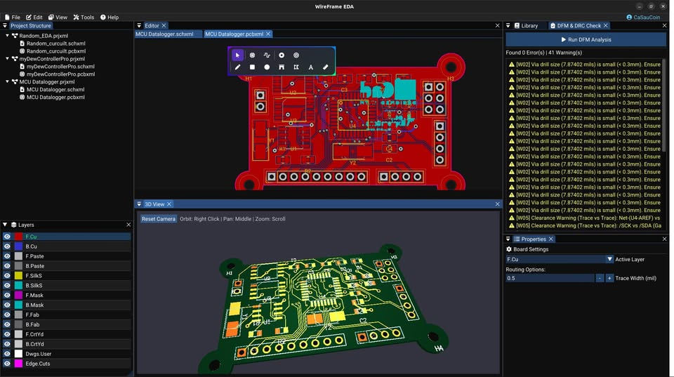
Main menus
File
Use File to:
- create a project, schematic, or PCB;
- open a WireFrame file or project;
- import a KiCad project or SVG board outline;
- save the active document;
- export schematic PDF, PCB PDF, or fabrication outputs;
- edit schematic page settings;
- close the document or project.
Commands that do not apply to the active document are disabled.
Edit
Use Edit for undo, redo, clipboard actions, selection operations, and other edits supported by the active editor. Prefer the displayed shortcut because key bindings can be customized.
View
Use View to show or hide:
- Project Structure;
- Editor Panel;
- Component Library;
- Properties;
- Local Library Manager;
- AI Copilot Chat;
- PCB Layers;
- Zone Manager;
- Design Rules.
Tools
Use Tools for the Symbol Library Editor, PCB Footprint Editor, schematic wiring assistance, Update Schematic to PCB, ERC, DFM/DRC, Fabrication Output, and Gerber Viewer. Availability depends on the active document.
Simulation
Use Simulation for the SPICE Simulation Panel, Pre-flight Validation Checklist, and SPICE Model Editor.
Preferences
Open the Preferences dialog to configure application, panel, grid, simulation, AI, and update settings. Use Reset to Default Layout only when you intend to discard the saved docking layout.
Help and account
Use the Help menu for documentation, downloads, feedback, updates, and About. The account area shows sign-in or subscription state and provides saved-login controls.
Docking layout
Drag a panel by its title to dock it to another edge or tab group. Preferences can enable detachable multi-monitor panels and companion-panel behavior.
Short video — Rearrange and restore panels
Video review needed
Replace the current clip if its View or Preferences labels are old. Show docking one panel, enabling or demonstrating a detachable panel, and restoring a saved/default layout. Duration: 12–18 seconds, 1080p.
Project Structure
The Project Structure panel lists the active project and linked schematics and PCBs. Use it to open documents and manage project membership. Standalone files appear separately from project-owned documents.
Image — Current Project Structure
Image review needed
Capture a current project tree with multiple schematics and one PCB. Replace older images if icons or group labels differ. Suggested size: 420 × 720 px.
Editor panel
The center editor displays the active schematic or PCB. Common actions include:
- mouse wheel to zoom;
- middle-drag or the configured pan action to move the view;
- click or box selection;
- context menu for object-specific actions;
- shortcuts shown in the active key map.
Toolbars change when switching between schematic and PCB documents.
Component Library
With a schematic active, the library lists symbols. With a PCB active, it lists footprints. Search before placing an item and check that the selected library item is the intended part or package.
Use View → Local Library Manager to add or remove persistent library sources.
Properties
Properties follow the current selection:
- schematic components expose value, footprint, and text attributes;
- wires and labels expose connectivity-related properties;
- PCB footprints expose placement, layer, designator, and model-related properties;
- traces, vias, zones, and graphics expose type-specific settings.
When multiple objects are selected, only shared or supported batch properties may be available.
PCB Layers
The PCB Layers panel controls active layer, visibility, and color. Hiding a layer changes the view, not the board data. Confirm the active copper layer before routing or adding vias.
Notifications and logs
Status messages and notification overlays report saves, imports, checks, and failures. Read the full message before repeating an action. For simulation, also inspect Last run and the simulation log.
Short video — Notification and status feedback
Video review needed
Capture one successful save/import notification and one non-destructive warning. Replace the existing clip if its overlay design is outdated. Duration: 8–12 seconds, 1080p.
Current Preferences categories
| Category | Includes |
|---|---|
| Application | Theme, units, autosave |
| Panels | Detachable panels, follow behavior, layouts and presets |
| Grid | Visibility, crosshair, snap, step, rotation, PCB defaults |
| Simulation | Engine paths, default analysis, transient defaults |
| AI | Provider key and model settings |
| About / Updates | Version, tier, update check |
Select OK to keep changes or Cancel to discard pending dialog changes.