Getting Started
This guide walks you through your first session with WireFrame EDA in approximately 10 minutes.
You will learn how to launch the application, understand the main interface, and set up your first project.
What you'll learn
- Launching WireFrame
- Understanding the main UI areas
- Creating a new project
- Adding schematic and PCB files
- Opening existing projects and files
1. Launching WireFrame
Run from terminal:
./wireframe
Open Start Menu → type WireFrame → press Enter.
Open Launchpad → find WireFrame → click to launch.
On startup, WireFrame automatically restores any open projects and documents from your previous session.
A brief dark flash is normal — the interface loads on the next render frame.
2. The Main Interface
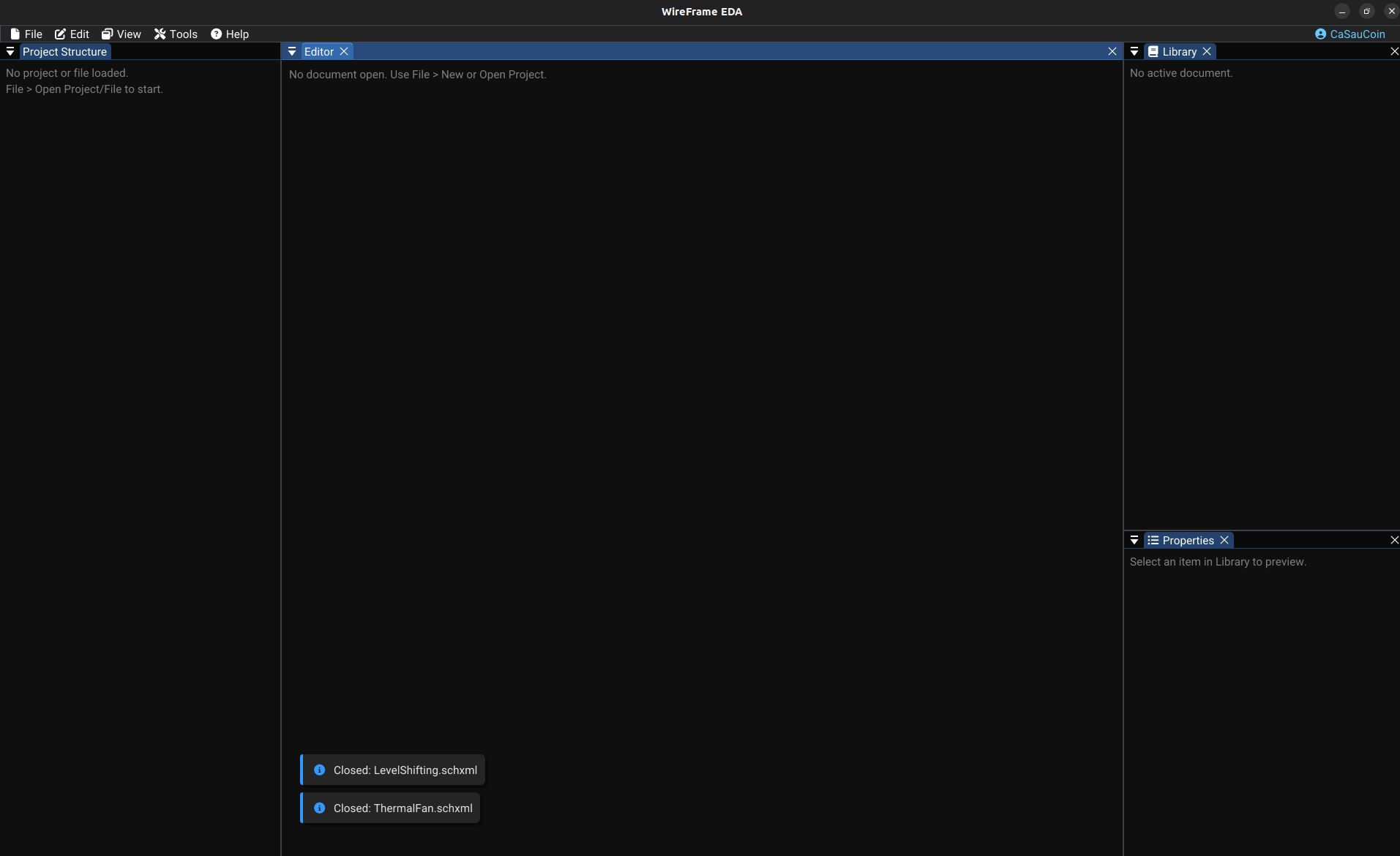
After launching, you will see the following layout:
| Area | Default position | Purpose |
|---|---|---|
| Menu bar | Top | Access all features via menus |
| Project Structure | Left | Project file tree |
| Canvas (Editor) | Center | Design area — schematic or PCB |
| Library | Right (top) | Component / footprint list |
| Properties | Right (bottom) | Edit properties of the selected object |
| Layer (PCB only) | Right (middle) | Toggle and select PCB layers |
| Logger | Bottom overlay | Errors, warnings, and status messages |
Rearranging panels
Drag any panel tab to a different edge or corner to reposition it. Your layout is saved automatically and restored on next launch.
3. Creating a New Project
Why use a project?
A project (.prjxml) is a central hub for all your files — schematics, PCBs, and libraries. Working inside a project makes file management easier and enables one-click Gerber export.
Steps:
- Go to File → New → New Project (.prjxml)
- Choose a folder and enter a filename, for example:
MyBoard.prjxml - Click Create (or Save)
WireFrame automatically creates:
MyBoard.prjxml— stores references to all schematics and PCBs- A
lib/folder for local libraries
The Project Structure panel immediately shows your new project with empty Schematics and PCBs groups.
4. Adding a Schematic File
- Go to File → New and choose a new schematic
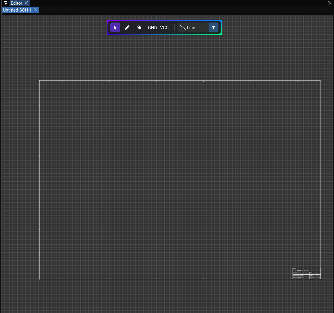
- A new tab opens in the editor:
Untitled-SCH-1 - The canvas shows:
- A dot grid on a dark background
- An A4 page outline
- The floating schematic toolbar at the top
Press Ctrl+S to save → name the file .schxml, for example: main.schxml
The schematic canvas looks like this:
5. Adding a PCB File
- Go to File → New and choose a new PCB
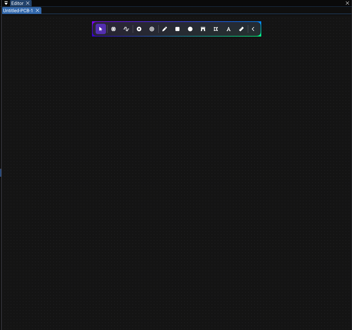
- A new tab opens:
Untitled-PCB-1 - The canvas shows a grid and the PCB floating toolbar
Convert from schematic instead
Rather than creating a PCB manually, complete your schematic first and use Tools → Update Schematic to PCB. Review the target board, imported footprints, and ratsnest before routing.
The PCB canvas looks like this:
6. Opening an Existing Project or File
Opening a project (.prjxml)
- File → Open Project (.prjxml)
- Select the
.prjxmlfile - The Project Structure panel populates with all linked schematics and PCBs
- Click any entry to open it in the editor
Opening a standalone file
- File → Open File (or Ctrl+O)
- Select a
.schxml(schematic) or.pcbxml(PCB) file - The file opens as a tab in the editor — no project required
Next Steps
You now know the basics. Continue with:
| Next page | Content |
|---|---|
| UI Overview | Detailed guide to every panel and toolbar |
| Schematic Editor | Place components, draw wires, manage nets |
| PCB Editor | Lay out footprints, route traces, export Gerbers |
| Full Tutorial | End-to-end walkthrough: a complete LED circuit |