Projects and Files
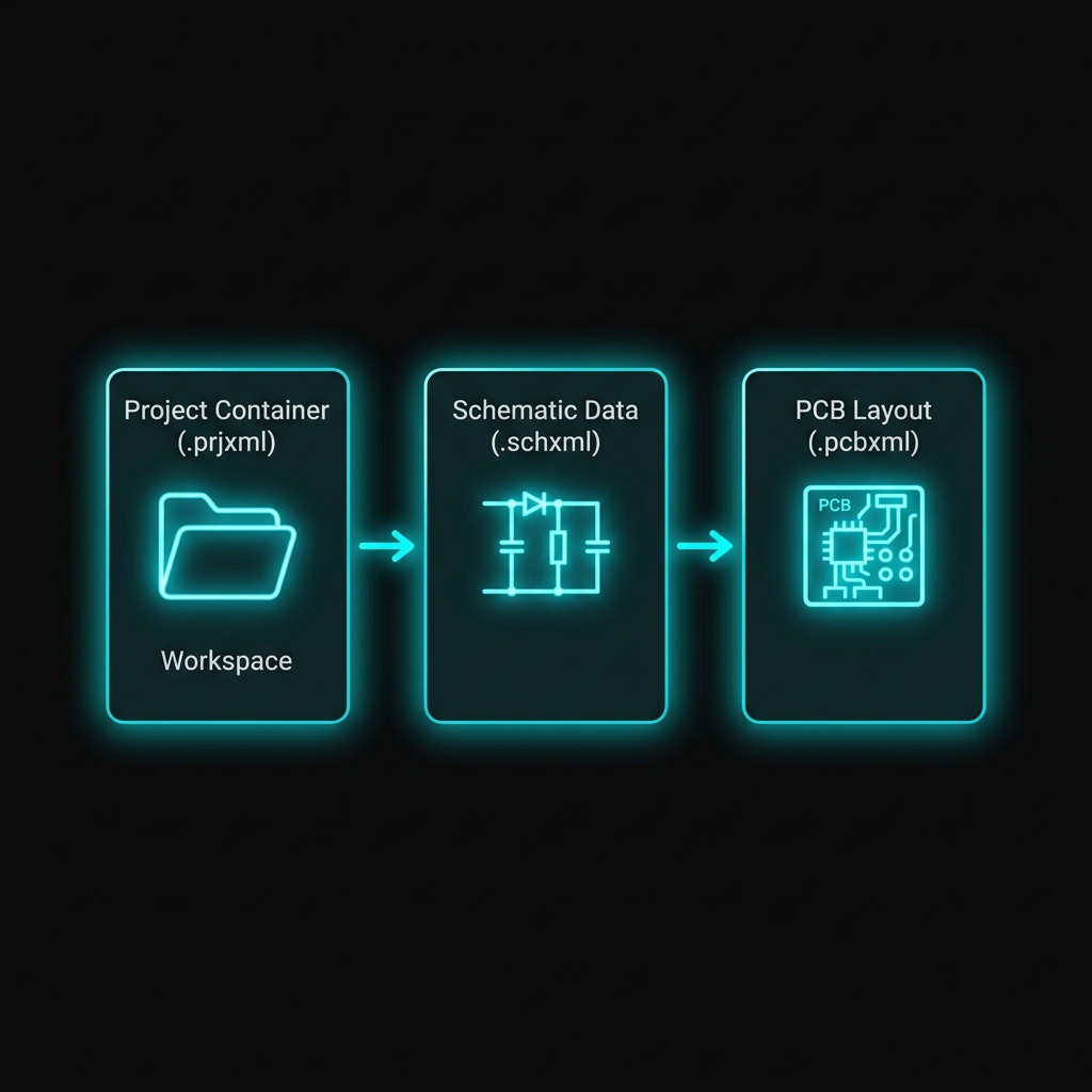
Use a WireFrame project to keep schematics, PCB documents, and project libraries together. A project can contain multiple schematics and PCBs, while a standalone document can be opened without joining a project.
Create a project
- Select File → New → New Project (.prjxml).
- Choose the parent folder.
- Enter the project name in the creation dialog.
- Select Create.
Keep the project and its documents in a dedicated folder. This makes relative library and model paths easier to move, archive, and share.
Short video — Create a new project
Video review needed
Replace or re-record the existing clip if its menu labels differ from File → New → New Project (.prjxml). Show folder selection, project naming, creation, and the new project in Project Structure. Duration: 10–15 seconds, 1080p.
Open a project or document
| What you want to open | Command |
|---|---|
| WireFrame project | File → Open Project (.prjxml) |
| Project, schematic, or PCB | File → Open File |
| KiCad project | File → Import → KiCad Project (.kicad_pro, .pro) |
Opening a .prjxml restores its linked documents and project structure. Opening a .schxml or .pcbxml directly adds it as a standalone file for the current session.
Image — Project Structure with multiple documents
Image review needed
Capture the current Project Structure panel with one project, at least two schematics, and one PCB. Replace the existing image if the icons, tree labels, or panel styling are from an older build. Suggested size: 420 × 720 px.
Add and organize documents
Use the Project Structure panel to add a new or existing schematic or PCB to the active project. Save a newly created document before relying on it as a project member.
| Document | Extension | Contains |
|---|---|---|
| Project | .prjxml |
Linked schematics, PCBs, and library references |
| Schematic | .schxml |
Symbols, wires, labels, annotations, and page settings |
| PCB | .pcbxml |
Footprints, nets, traces, vias, zones, layers, and design rules |
Use File → Save for the active document and File → Save As when you need a new path. Closing a project does not delete its documents.
Update a schematic to PCB
Before updating a PCB:
- Complete the schematic connectivity.
- Assign a valid footprint to every physical component.
- Run ERC and resolve critical issues.
- Select Tools → Update Schematic to PCB.
- Choose the target PCB when the project has more than one.
- Review new or changed footprints and the ratsnest before routing.
Footprints are required
A physical component without a valid footprint cannot be placed correctly on the PCB. Resolve missing symbols, footprints, and pin-count mismatches in Component Review or the library editors before continuing.
Short video — Update schematic to PCB
Video review needed
Re-record the existing conversion clip because the current command is Tools → Update Schematic to PCB, not “Project → Convert to PCB.” Show target selection, the PCB opening, footprints, and ratsnest. Duration: 15–20 seconds, 1080p.
Import a KiCad project
- Select File → Import → KiCad Project (.kicad_pro, .pro).
- Select the KiCad project file.
- Keep WireFrame open while the progress overlay reports each import stage.
- Review the resulting project, schematics, PCB, and library assignments.
- Save the converted WireFrame documents.
After import, check:
- sheet and document count;
- symbol values and references;
- net labels, power symbols, and connectivity;
- footprint side, rotation, and pad numbering;
- board outline, zones, vias, and design rules;
- library and 3D model paths.
Short video — Import a KiCad project
Video review needed
Replace the current clip if it does not show the asynchronous progress overlay. Capture file selection, at least two progress stages, the imported Project Structure, and one opened document. Duration: 15–25 seconds, 1080p.
Import scope and removed legacy guidance
The current project importer supports KiCad .kicad_pro and legacy .pro project files. Older guideline sections claiming File → Import → Altium Project or Eagle Project have been removed because those commands are not present in the current application.
Altium library files remain supported through View → Local Library Manager. See Library Import and Management.
Import a PCB outline
With a PCB active, select File → Import → CAD Outline (.svg). Review scale, placement, and whether the imported geometry belongs on the intended board-outline layer before routing or fabrication.
Note
The current file picker accepts SVG for this command. Do not document DXF as supported until it is selectable and verified in a release build.
Session restoration
WireFrame remembers open projects, standalone documents, panel layout, and recent folders. On the next launch, confirm that restored documents still resolve their linked libraries and models.
If the previous session should not be restored, close its documents and project before exiting or reset the saved layout/session from Preferences.