PCB Editor — Overview
The PCB Editor handles board layout — from component placement to trace routing, copper zones, design rule checks, and manufacturing file export.
What You Can Do Here
| Task | Tool |
|---|---|
| Place footprints from library or schematic | Library panel / Available Footprints dialog |
| Route copper traces between pads | Route Trace tool (X) |
| Place vias to switch routing layers | Via tool (V) |
| Add mechanical holes (screws, standoffs) | Place Hole tool |
| Define the board outline | Edge.Cuts layer + drawing tools |
| Fill copper zones (ground planes) | Zone / Fill GND Plane |
| Run DFM / DRC checks | Tools → DFM & DRC Check Panel |
| Export Gerber, drill, BOM, PDF | File → Export → Fabrication Outputs / Tools → Fabrication Output |
| Preview the board in 3D | View → 3D Viewer |
Workspace
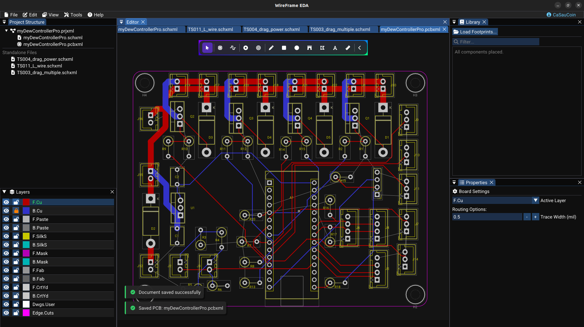
- Canvas — the board area with grid, footprints, traces, zones, and ratsnest lines (unrouted connections)
- Toolbar — floating tool buttons above the canvas
- Layer panel — toggle visibility and select the active routing layer
- Library panel — footprint list for placement
- Properties panel — edit properties of the selected PCB object
PCB Toolbar Tools
| Tool | Shortcut | Function |
|---|---|---|
| Select | Esc | Select and move objects |
| Place Footprint | — | Place a footprint from the library |
| Route Trace | X | Route copper traces between pads |
| Draw Via | V | Place a via manually |
| Place Hole | — | Place a mechanical hole |
| Draw Line / Rect / Circle / Arc / Polygon | — | Draw graphic shapes on any layer |
| Draw Text | — | Place text on silkscreen or fab layers |
| Measure | — | Measure distances on the board |
Board Outline (Edge.Cuts)
Every PCB needs a board outline that defines its physical shape:
- In the Layer panel, click Edge.Cuts to make it the active layer
- Use the Draw Rectangle (or Polygon) tool to draw the board shape
- The outline appears in magenta
Why Edge.Cuts matters
The board outline is used for: - Telling the manufacturer where to cut the board - Defining the valid placement area for footprints (DFM checks this) - Clipping copper zone fills at the board edge
Ratsnest Lines
Ratsnest lines are thin dashed lines showing connections that have not yet been routed:
Short video — Ratsnest cleared by routing
Video needed
Record 10–15 seconds showing one ratsnest connection before routing, the completed track, and the ratsnest update. The existing video file is empty and must be replaced.
- Ratsnest lines automatically update after every edit
- When you route a trace, the corresponding ratsnest line disappears
- The goal is to route until all ratsnest lines are gone
Section Pages
| Page | What you'll learn |
|---|---|
| Footprints & Placement | Load libraries, place and arrange footprints |
| Routing | Route traces, vias, mechanical holes |
| Layers & Views | Layer management, visibility, navigation |
| Zones & Planes | Copper fills, ground planes, zone priority |
| Design Rules & Net Classes | Clearance, trace width, via size, net class configuration |
| DFM & DRC | Design rule and manufacturability checks |
| Fabrication & Export | Gerber, drill, BOM, PDF export |
Related Sections
| Section | What you'll learn |
|---|---|
| 3D Viewer | Preview the PCB with 3D component models |
| Placement and Routing Assistant | Review AI-assisted placement and routing proposals |